Scaling the AI Data Center: Silicon Photonics as the Industrial Foundation for Next-Gen Optics
In the world of optical transceivers, a common question is: “Which is better—electro-absorption modulated laser (EML) or silicon photonics?” It is a useful question for understanding where high-speed optical networking is heading. The short answer is that both technologies have played important roles in the evolution of high-speed optics. AOI has built products using each and was among the first companies to bring EML technology to market. Today, however, much of AOI’s roadmap—from 400G to 800G to 1.6T—is centered on silicon photonics. Not because it is trendy, but because it provides a stronger foundation for scaling and automation.
What is EML Technology?
EML technology combines a laser and a modulator into a single device. This architecture allows high-speed optical signals to be generated within a compact component. Its integrated structure simplified early product development and helped accelerate the introduction of faster optical modules.
EML technology continues to be the "gold standard" for specific applications, particularly long-reach (LR4/ER4) requirements exceeding 10km. Because of its superior "chirp" and dispersion characteristics, EML remains a strong fit where established architectures or specialized long-distance system requirements are the priority.
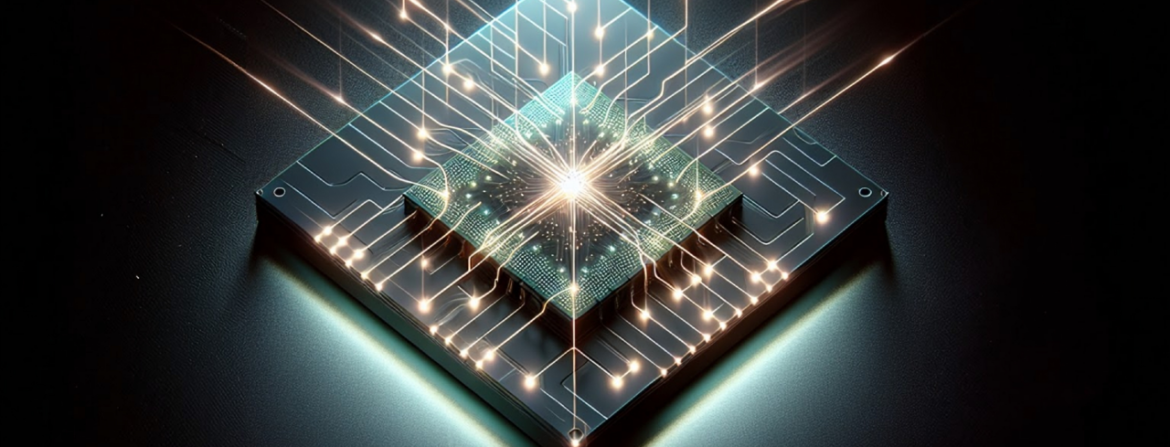
What is Silicon Photonics?
Silicon photonics uses silicon and CMOS-style manufacturing processes to build optical components on a chip. A continuous-wave laser feeds the photonic integrated circuit (PIC), which performs modulation, routing, and other optical functions. This design enables a highly integrated optical platform. Because silicon photonics leverages semiconductor manufacturing techniques, it is well suited to support the growing scale of cloud data centers, AI infrastructure, and high-bandwidth networking environments.
Silicon Photonics and the Future of High-Speed Optics
As networking speeds advance from 400G to 800G and eventually 1.6T optical transceivers, scalability becomes increasingly important. Silicon photonics enables multiple product generations to be built on a shared platform, allowing core design elements and manufacturing processes to evolve more efficiently over time. This platform continuity helps streamline the development of new optical modules while supporting more predictable product roadmaps. For hyperscale data centers and network operators, this consistency can simplify infrastructure planning as network speeds continue to increase.
From a performance standpoint, while silicon photonic modulators may have different insertion loss profiles compared to EML, they are the primary enablers for next-generation, low-power architectures. This design flexibility allows for the reduction of overall system power consumption (W/bit) by streamlining the optical path and reducing the reliance on power-intensive signal processing components—a critical requirement for the energy-demanding environments of modern AI data centers.
Why AOI’s Roadmap Leans to Silicon Photonics
One advantage of silicon photonics is its compatibility with automated manufacturing processes. Rather than redesigning the manufacturing flow for each new speed generation, AOI can carry the same core platform forward from 400G to 800G and beyond. That consistency benefits both engineering teams and customers seeking predictable product ramps and stable roadmaps.
The technology also lends itself naturally to automation. Its chip-level integration makes assembly steps more repeatable, which translates into higher yields and faster, more reliable scaling. This is a key factor in AOI’s ability to produce optical components economically at high volume, including in the United States, where automated manufacturing supports shorter and more resilient supply chains.
The Next Generation of Optical Connectivity
EML continues to have a role in the optical ecosystem, but its role has evolved. Earlier product cycles relied heavily on EML technology because it enabled faster time-to-market. However, as we move toward 1.6T, EML faces a "complexity wall". An 8-channel 1.6T EML module requires eight separate laser chips to be Individually aligned and bonded—a process prone to "yield stacking" risks. Silicon photonics avoids this by using monolithic integration, where one photonic chip handles all channels.
Furthermore, silicon photonics is the primary driver behind the transition to CPX (Common Pluggable) platforms and External Laser (ELSFP) architectures. By moving heat-generating lasers away from the sensitive high-density optics and switch ASICs, this approach solves the thermal challenges of modern AI clusters. This "remote laser" design ensures that as we scale to higher bandwidths, the most critical components remain in a stable thermal environment, significantly improving overall system reliability and serviceability.
As AI infrastructure and high-performance computing continue to expand, the industry will increasingly rely on technologies that enable scalable and automated production. With its ability to support these demands, silicon photonics is well positioned to drive the next era of high-speed connectivity.